|
联系我们
|
| 地 址:深圳市福田保税区英达利数码科技园B座 |
| 邮 编:518033 |
| 联系人:刘先生 |
| 电 话:0755-82838457 |
| 传 真:0755-25331367 |
| 邮 箱:jinyi886@qq.com |
|
|
|
|
|
|
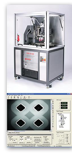
DDR200 NIRMcBain高速缺陷检测仪DDR200 NIR
|
|
|
|
公司名称:
香港金溢科技有限公司
|
|
参考价格:
0
元
|
|
发布时间:
2010-12-13
|
| 产品描述: |
测试半导体产品测试仪美国McBain
1.. McBain DDR200 NIR and DDR300 NIR
Near Infrared Subsurface Defect Detection and Review Systems
The McBain DDR200 NIR (for 200mm) and DDR300 NIR (for 300mm) provide high-speed defect detection and precision measurement on wafers and other parts. These cost-efficient systems offer unique advantages for both production and process development use, providing an optimum near-infrared (900-1700nm) solution when both subsurface defect detection and dimensional metrology are required.
These DDR systems feature a powerful set of automated and semi-automated optical and digital video tools, which are optimized for high accuracy, production throughput and ease of use. The automated and versatile platform features McBain"s state-of-the-art near-infrared Koehler Epi-illumination as well as optional transmitted-illumination packages. All systems are configured on McBain Systems" precision multi-axis platforms.
Applications
· For in-process, post-process and failure analysis
· Bonded wafer alignment
· Die alignment (flip-chip or hybridization)
· Subsurface defect visualization, detection, characterization
· MEMS device inspection and metrology
· 3D stacking process development and control
Key Features
Designed for automatic / semiautomatic operation
· Extensive defect detection features and capability
· Integrated dimensional metrology features
· Able to penetrate thicker materials, more highly doped materials and rougher surfaces than other systems
· Submicron-precision optical measurements
· High-accuracy staging, to 20nm linear encoder resolution
· Highest resolution 900-1700nm InGaAs digital camera in class
· High-speed linear servo motor staging
· 50-500 defects/measurement/second per field of view, typical
· Very easy to use, program and set up
· Multiple wafer/die/part handling systems available
· Application-specific customizable software
· Semi Standard S2/S8 compliant
·
--------------------------------------------------------------------------------------------
2 . McBain DDR200 and DDR300
200mm and 300mm Defect Detection and Review Systems
Download Brochure PDF
Request a Quotation <mailto:sales@mcbainsystems.com>
The McBain DDR200 and DDR300 for 200mm and 300mm wafer defect detection and review are unmatched in value and features in this special application and price category. The systems offer significant and unique advantages for both production and engineering use, and provide an ideal solution when both defect detection and dimensional metrology are required. They can be used as dedicated production tools or as versatile process development tools.
Key Features
· 200mm or 300mm X-Y stage
· BF/DF (standard), Nomarski (optional), UV and IR versions available
· Defect detection, classification and review (review-only optional)
· Reflected light (standard), transmitted light for mask inspection (optional)
· Video autofocus (standard), laser autofocus (optional)
· McBain Ergo workstation (standard), TMC isolation workstation (optional)
· McBain lead screw/universal nut driven cross roller bearing stage, or
· McBain high-speed linear motor stage
· Monochrome or color 5-megapixel digital camera
· Wafer- and mask-loading options available
· Standard working distance, long working distance and super-long working distance objectives
· 2x, 5x, 10x, 20x, 50x, 100x, 150x, 200x objectives (20x to 2000x magnification)
· 6 inches of vertical travel
· Manual or motorized X, Y, Z, and theta axis options
--------------------------------------------------------------------------------------------
3 . McBain MMS200
Fully Automatic Mask Alignment Microscope and Handling System
The McBain MMS200 is the affordable solution for small-field, g-line, sub-micron stepping mask alignment. Used extensively in thin film head production and micromachining/MEMS fabrication, it is the ideal photolithography tool for maximizing throughput while minimizing production costs. It is available with manual or motorized options for loading/unloading masks and sliders.
Key Features
· Small field g-line stepper (436nm exposure)
· Vision and alignment at 546nm
· 5:1 mask reduction ratio
· Apochromatic lens NA: 0.2
· 1000W HgXe illuminator
· FOV: 20mm x 20mm
· Resolution: 1.7μm
· 6” x 6” mask holder
· Split-field camera machine vision system
· 4 motorized axes for alignment and motion: X,Y,Z and theta
· Large depth of focus: 5.4 μm
· Manual or motorized options for load and unload of mask and sliders
· Designed for serviceability and minimum footprint
· SECS/GEM interface
· Configurable product parameters:
· Slider width and length
Slider rows and columns
Exposure area rows and columns
Target spacing
Post-align offsets
Exposure dosage
Graphic site selections
Control components have individually accessible dialogs for troubleshooting and maintenance
------------------------------------------------------------------------------------------------------
4. McBain NIR 200 Near Infrared Inspection System
Fully-automatic Measuring and Alignment Microscope and Handling System
The McBain NIR 200 is a fully-automated near-infrared inspection system for extracting wafers from a source cassette and measuring multiple alignment targets with 0.5 micron repeatability. The tool can be run in manual, local auto or full remote through GEM/SECS.
The NIR200 is a reliable production tool that is highly configurable to end-user needs. Throughput is partly dependent on the number of sites per wafer; a nine-site inspection set-up can run a cassette of 25 wafers in 45 minutes. The NIR200 is best-in-class for wafer-to-wafer and die-to-die critical alignment measurement and verification. This unique tool has been sold into many industries and a range of applications including sub-surface wafer and die inspection for cracks and bond integrity, MEMS, wafer bonding, 3-D chip stacking, failure analysis, process development, tool verification, part characterization, environmental testing and more.
See also the semi-automatic version of this tool.
Key Features
Automatic loading and unloading of 4", 6" and 8" wafers
Motorized X, Y, Z and theta axis
900nm to 1700nm custom optical system provides best-in-class NIR visibility
Highly sensitive InGaAs camera
Integrated vision system and customizable software for:
Image optimization
Part recipe
Palletization
Critical measurements
Defect detection and classification
6 inches of vertical Z travel allows custom tooling
6", 8" or 12" travel XY stage options
solid reflected or transmitted light
manual coarse, fine or motorized options
0.5 micron feature resolution
0.1 micron positioning accuracy and repeatability
Turnkey integrated motion control packages
Ergonomic 3 axis joystick and trackball controls
Vibration isolation
Custom configurations available
5.McBain Z-NIR Near Infrared Inspection System
Semi-automatic Measuring and Alignment Microscope
Download Brochure PDF <http://www.mcbaininstruments.com/pdf/Infrared_Inspection_Systems_broch.pdf>
Request a Quotation <mailto:sales@mcbainsystems.com>
The McBain Z-NIR Near Infrared Inspection System is best-in-class for wafer-to-wafer and die-to-die alignment measurement and verification. This unique tool has been sold into many industries with various applications including sub-surface wafer and die inspection for cracks and bond integrity, MEMS, wafer bonding, 3-D chip stacking, failure analysis, process development, tool verification, part characterization, environmental testing and more.
See also the fully-automated version of this tool.
Key Features
900nm to 1700nm custom optical system provides best-in-class NIR visibility
Highly sensitive InGaAs camera
Integrated vision system and customizable software for:
Image optimization
Part recipe
Palletization
Critical measurements
Defect detection and classification
6 inches of vertical Z travel allows custom tooling
Manual or motorized systems available
6", 8" or 12" travel XY stage options
solid reflected or transmitted light
manual coarse, fine or motorized options
0.5 micron feature resolution
0.1 micron positioning accuracy and repeatability
Turnkey integrated motion control packages
Ergonomic 3 axis joystick and trackball controls
Vibration isolation
Custom configurations available |

|
|
|
| |
| |
DDR200 NIRMcBain高速缺陷检测仪DDR200 NIR的详细介绍
测试半导体产品测试仪美国McBain
1.. McBain DDR200 NIR and DDR300 NIR
Near Infrared Subsurface Defect Detection and Review Systems
The McBain DDR200 NIR (for 200mm) and DDR300 NIR (for 300mm) provide high-speed defect detection and precision measurement on wafers and other parts. These cost-efficient systems offer unique advantages for both production and process development use, providing an optimum near-infrared (900-1700nm) solution when both subsurface defect detection and dimensional metrology are required.
These DDR systems feature a powerful set of automated and semi-automated optical and digital video tools, which are optimized for high accuracy, production throughput and ease of use. The automated and versatile platform features McBain"s state-of-the-art near-infrared Koehler Epi-illumination as well as optional transmitted-illumination packages. All systems are configured on McBain Systems" precision multi-axis platforms.
Applications
· For in-process, post-process and failure analysis
· Bonded wafer alignment
· Die alignment (flip-chip or hybridization)
· Subsurface defect visualization, detection, characterization
· MEMS device inspection and metrology
· 3D stacking process development and control
Key Features
Designed for automatic / semiautomatic operation
· Extensive defect detection features and capability
· Integrated dimensional metrology features
· Able to penetrate thicker materials, more highly doped materials and rougher surfaces than other systems
· Submicron-precision optical measurements
· High-accuracy staging, to 20nm linear encoder resolution
· Highest resolution 900-1700nm InGaAs digital camera in class
· High-speed linear servo motor staging
· 50-500 defects/measurement/second per field of view, typical
· Very easy to use, program and set up
· Multiple wafer/die/part handling systems available
· Application-specific customizable software
· Semi Standard S2/S8 compliant
·
--------------------------------------------------------------------------------------------
2 . McBain DDR200 and DDR300
200mm and 300mm Defect Detection and Review Systems
Download Brochure PDF
Request a Quotation <mailto:sales@mcbainsystems.com>
The McBain DDR200 and DDR300 for 200mm and 300mm wafer defect detection and review are unmatched in value and features in this special application and price category. The systems offer significant and unique advantages for both production and engineering use, and provide an ideal solution when both defect detection and dimensional metrology are required. They can be used as dedicated production tools or as versatile process development tools.
Key Features
· 200mm or 300mm X-Y stage
· BF/DF (standard), Nomarski (optional), UV and IR versions available
· Defect detection, classification and review (review-only optional)
· Reflected light (standard), transmitted light for mask inspection (optional)
· Video autofocus (standard), laser autofocus (optional)
· McBain Ergo workstation (standard), TMC isolation workstation (optional)
· McBain lead screw/universal nut driven cross roller bearing stage, or
· McBain high-speed linear motor stage
· Monochrome or color 5-megapixel digital camera
· Wafer- and mask-loading options available
· Standard working distance, long working distance and super-long working distance objectives
· 2x, 5x, 10x, 20x, 50x, 100x, 150x, 200x objectives (20x to 2000x magnification)
· 6 inches of vertical travel
· Manual or motorized X, Y, Z, and theta axis options
--------------------------------------------------------------------------------------------
3 . McBain MMS200
Fully Automatic Mask Alignment Microscope and Handling System
The McBain MMS200 is the affordable solution for small-field, g-line, sub-micron stepping mask alignment. Used extensively in thin film head production and micromachining/MEMS fabrication, it is the ideal photolithography tool for maximizing throughput while minimizing production costs. It is available with manual or motorized options for loading/unloading masks and sliders.
Key Features
· Small field g-line stepper (436nm exposure)
· Vision and alignment at 546nm
· 5:1 mask reduction ratio
· Apochromatic lens NA: 0.2
· 1000W HgXe illuminator
· FOV: 20mm x 20mm
· Resolution: 1.7μm
· 6” x 6” mask holder
· Split-field camera machine vision system
· 4 motorized axes for alignment and motion: X,Y,Z and theta
· Large depth of focus: 5.4 μm
· Manual or motorized options for load and unload of mask and sliders
· Designed for serviceability and minimum footprint
· SECS/GEM interface
· Configurable product parameters:
· Slider width and length
Slider rows and columns
Exposure area rows and columns
Target spacing
Post-align offsets
Exposure dosage
Graphic site selections
Control components have individually accessible dialogs for troubleshooting and maintenance
------------------------------------------------------------------------------------------------------
4. McBain NIR 200 Near Infrared Inspection System
Fully-automatic Measuring and Alignment Microscope and Handling System
The McBain NIR 200 is a fully-automated near-infrared inspection system for extracting wafers from a source cassette and measuring multiple alignment targets with 0.5 micron repeatability. The tool can be run in manual, local auto or full remote through GEM/SECS.
The NIR200 is a reliable production tool that is highly configurable to end-user needs. Throughput is partly dependent on the number of sites per wafer; a nine-site inspection set-up can run a cassette of 25 wafers in 45 minutes. The NIR200 is best-in-class for wafer-to-wafer and die-to-die critical alignment measurement and verification. This unique tool has been sold into many industries and a range of applications including sub-surface wafer and die inspection for cracks and bond integrity, MEMS, wafer bonding, 3-D chip stacking, failure analysis, process development, tool verification, part characterization, environmental testing and more.
See also the semi-automatic version of this tool.
Key Features
Automatic loading and unloading of 4", 6" and 8" wafers
Motorized X, Y, Z and theta axis
900nm to 1700nm custom optical system provides best-in-class NIR visibility
Highly sensitive InGaAs camera
Integrated vision system and customizable software for:
Image optimization
Part recipe
Palletization
Critical measurements
Defect detection and classification
6 inches of vertical Z travel allows custom tooling
6", 8" or 12" travel XY stage options
solid reflected or transmitted light
manual coarse, fine or motorized options
0.5 micron feature resolution
0.1 micron positioning accuracy and repeatability
Turnkey integrated motion control packages
Ergonomic 3 axis joystick and trackball controls
Vibration isolation
Custom configurations available
5.McBain Z-NIR Near Infrared Inspection System
Semi-automatic Measuring and Alignment Microscope
Download Brochure PDF <http://www.mcbaininstruments.com/pdf/Infrared_Inspection_Systems_broch.pdf>
Request a Quotation <mailto:sales@mcbainsystems.com>
The McBain Z-NIR Near Infrared Inspection System is best-in-class for wafer-to-wafer and die-to-die alignment measurement and verification. This unique tool has been sold into many industries with various applications including sub-surface wafer and die inspection for cracks and bond integrity, MEMS, wafer bonding, 3-D chip stacking, failure analysis, process development, tool verification, part characterization, environmental testing and more.
See also the fully-automated version of this tool.
Key Features
900nm to 1700nm custom optical system provides best-in-class NIR visibility
Highly sensitive InGaAs camera
Integrated vision system and customizable software for:
Image optimization
Part recipe
Palletization
Critical measurements
Defect detection and classification
6 inches of vertical Z travel allows custom tooling
Manual or motorized systems available
6", 8" or 12" travel XY stage options
solid reflected or transmitted light
manual coarse, fine or motorized options
0.5 micron feature resolution
0.1 micron positioning accuracy and repeatability
Turnkey integrated motion control packages
Ergonomic 3 axis joystick and trackball controls
Vibration isolation
Custom configurations available
|
|
|
|